PCB reduces antenna size
In the area of PCB design, there are many different components that are critical to the overall success of a particular circuit. One of the most important of these components is the antenna, which is responsible for transmitting and receiving signals in a variety of different applications. However, when it comes to designing a PCB that includes an antenna, it can be a challenge to ensure that the size of the antenna meets the specifications of the overall system. In this article, we will explore some of the different techniques that can be used to shrink the size of PCB antennas, in order to ensure that they fit the necessary design parameters.
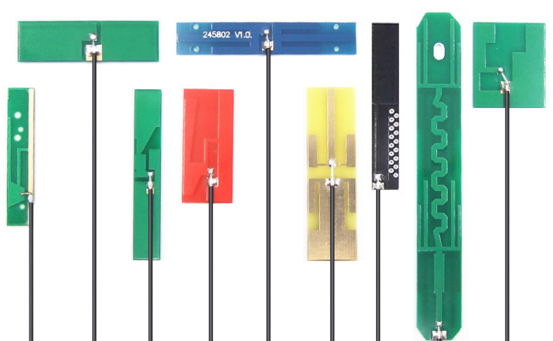
One of the most common techniques for shrinking the size of a PCB antenna is to use a different type of antenna altogether. For example, there are several types of antennas that are not physically connected to the PCB board itself, which can greatly reduce the overall size of the antenna. These can include patch antennas, which are thin, rectangular antennas that are mounted on a separate substrate, or even chip antennas, which are miniature antennas that can be soldered directly onto the PCB board.
Another technique that can be used to shrink the size of a PCB antenna is to adjust the shape and dimensions of the antenna itself. For example, by changing the length or width of the antenna, it is possible to alter the frequency response of the antenna in such a way that it can still transmit and receive signals effectively, while occupying less space on the board. Additionally, using specialized software tools, engineers can optimize the shape and design of the antenna for a particular range of frequencies or other characteristics, in order to ensure that it performs optimally.
Another option for shrinking the size of a PCB antenna is to use specialized materials or manufacturing techniques. For example, some antennas can be built using microstrip manufacturing techniques, which involve printing the antenna pattern onto a thin layer of copper or other conductive material, and then applying a dielectric substrate on top of it. This can greatly reduce the overall size of the antenna, and also improve its performance in terms of signal strength and frequency response.
Ultimately, there are a wide range of different techniques that can be used to shrink the size of PCB antennas, depending on the specific needs and requirements of a particular design. By carefully considering the different options available, and working with an experienced PCB design team, it is possible to develop antennas that are both small in size and highly effective in their performance. Whether it involves using different types of antennas, adjusting the shape and design of existing antennas, or employing specialized materials and manufacturing processes, there are many effective ways to achieve the desired result.
